
Jeremy has over 17 years of engineering and innovation experience. He has a Master's Degree in Electrical Engineering with an emphasis in Digital Signal Processing. He has been a member of IEEE for over 17 years and was elevated to the Senior Member grade in November 2011.
Test & Measurement Equipment
I have had the pleasure of working for many years on the development of a wide array of test and measurement equipment, which includes the following:
- 3.6 Gb/s, 13 Gb/s, and 50 Gb/s Bit Error Ratio Testers - Agilent Technologies, 2000-2002
- Jeremy's Error Tester (JET) 1.25 Gb/s Error Generation Instrument - Agilent Technologies, 2000-2002
- N1016A-K99 IEEE 802.3ae 10 Gigabit Ethernet Stressed Eye Test Set - Agilent Technologies, 2002
- N1015A Modulation Test Set - Agilent Technologies, 2002
- N9010A EXA, N9020A MXA, and N9030A PXA X-Series Spectrum Analyzers - Agilent Technologies, 2004-2007
- TG1C1A 13.5 GHz Clock Synthesizer - Centellax, 2007
- TG1B1A 12.5 Gb/s Serial Bit Error Ratio Tester - Centellax, 2007
- PPG12500 12.5 Gb/s Programmable Pattern Generator - Centellax, 2007-2012
- PED12500 12.5 Gb/s Programmable Error Detector - Centellax, 2007-2012
- PG32A (N4951A), PG32DE (N4951B-D32), PG32HV (N4951B-H32) 32 Gb/s Programmable Pattern Generator - Centellax, 2007-2012
- ED32A (N4952A) 32 Gb/s Programmable Error Detector - Centellax, 2007-2012
- SSB16000 (N4960A) 32 Gb/s Stressed Serial Bit Error Ratio Tester - Centellax, 2007-2012
- M8020A J-BERT High-Performance 16 Gb/s Bit Error Ratio Tester - Agilent Technologies, 2013
My involvement with the development of these instruments has spanned the system level architecture, control FPGA design, high-speed digital FPGA design, printed circuit board design, high-level software algorithm development, embedded control software, digital signal processing, manufacturing, design for manufacturing, test executive software development and EMI/EMC compliance testing.
I had many great mentors while working on each of these projects, and worked with a lot of very talented engineers and project managers. One of the reasons I enjoyed developing test and measurement equipment, aside from the technical side, was that I found it very fulfilling to be a part of the creation of equipment that is used and trusted by so many engineers across the globe in any number of applications requiring either optical or electrical testing. These types of products tend to have a very long life, and your work can sometimes out live you or your professional career. That's also pretty cool!
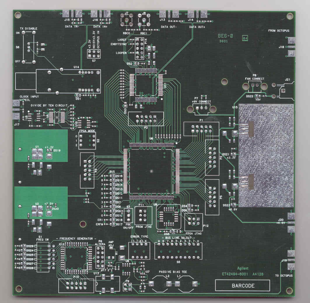
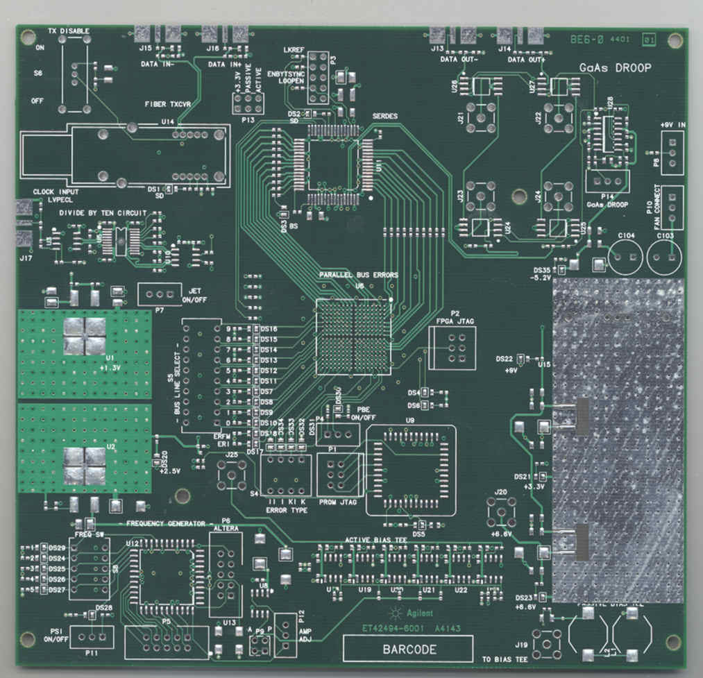
One of the first printed circuit boards I designed out of college was for the JET project. The pictures below show the board blank or solder sample for the first revision (left) and final revision (right) of the JET instrument's main printed circuit board. I learned a tremendous amount about designing printed circuit boards on the JET project. One of the most important things I learned was how to work with and manage the layout of the printed circuit board when working with a printed circuit board designer, otherwise known as a layout designer.
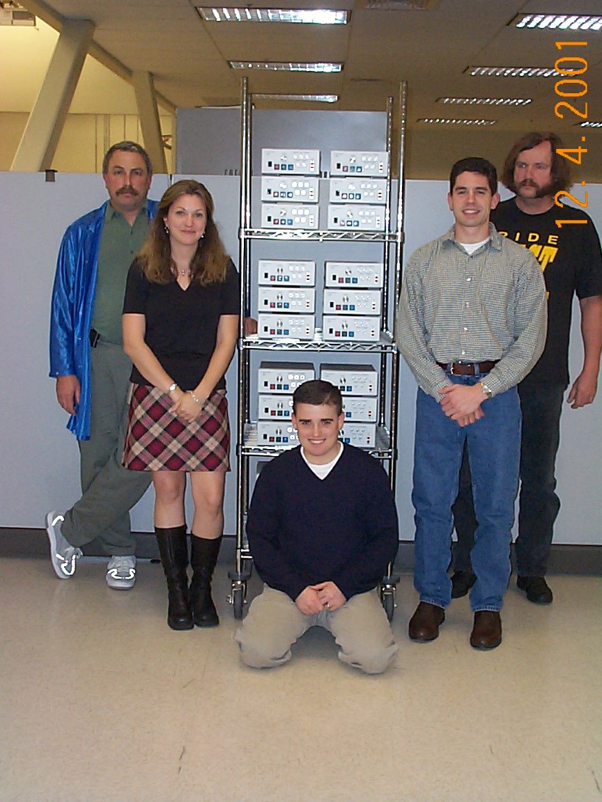
The JET project was my first project and I was able to experience the full product life cycle from requirements generation, ideation and block diagram design, printed circuit board and FPGA/CPLD design, mechanical enclosure design, design for manufacturing and test, and product documentation. Me and my team built 35 JET instruments and delivered them to the Agilent Technologies, now Keysight Technologies, Lightwave Division Marketing team for use during the sales execution of the 86130A 3.6 Gb/s Serial Bit Error Ratio Tester in December 2001. Below is a picture of the final assembly of the JET instruments. I'm the handsome fellow kneeling on the ground.
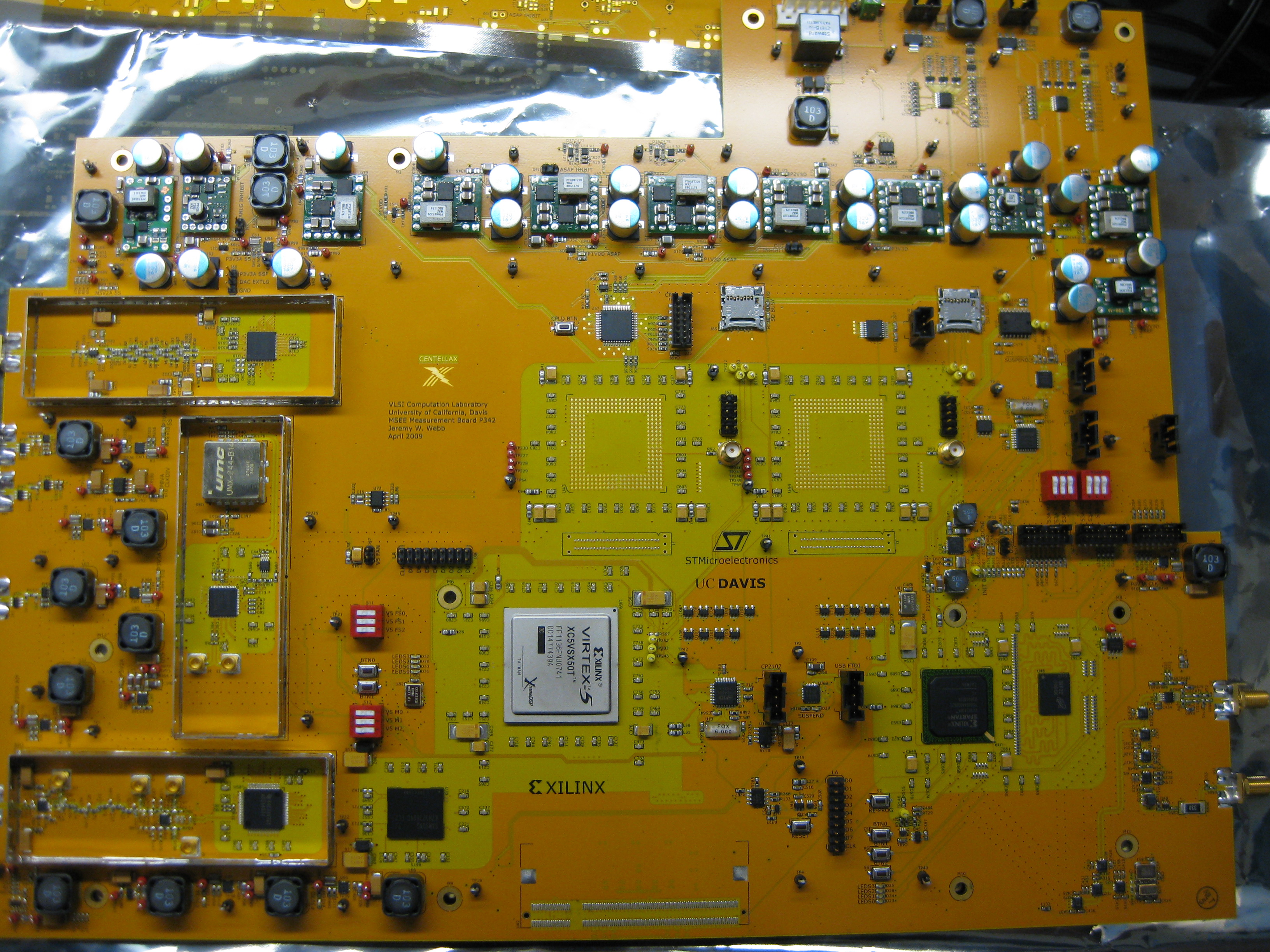
One of the later boards I designed was for my Master's Thesis Project, which was a DC - 120 MHz Spectrum Analyzer and Arbitrary Waveform Generator. A picture of the loaded printed circuit board is shown below. As expected, there's quite a large difference between the complexity of my first board (July 2001) and one of my latter printed circuit boards (April 2009).
 Back to Top
FPGA Development
Field programmable gate array (FPGA) and complex programmable logic device (CPLD) development has been a common theme in my career. I have had the opportunity to develop applications that target FPGAs and CPLDs using most register transfer languages (RTL), such as AHDL, VHDL, Verilog HDL, and SystemVerilog, and even some legacy schematic tools (i.e., Altera MAX+PLUS II). The first FPGA I targeted was a Xilinx Spartan-II (XC2S100-6FG256C), which was used in the JET project listed above to inject errors into the high-speed data path. The JET project also employed an Altera MAX CPLD to inject noise onto the power supply of the 1.25 Gb/s optical transceiver. Information about the JET project can be found in the paper entitled Agilent 86130A BitAlyzer Error Analysis Demonstration.
My FPGA designs have spanned control FPGA design, high-speed digital FPGA design, digital signal processing, and video signal processing. The control FPGA designs typically involved controlling external devices via a serial peripheral interface (SPI), inter-integrated circuit (I2C) interface, RS-232, USB, or parallel/discrete signal interface. Some designs employed an embedded soft-core processor, such as the Xilinx PicoBlaze or MicroBlaze, to orchestrate the higher level control of an embedded system.
Back to TopFull Stack Web Development/Back-end Database Development
I like Full Stack Web Development/Back-end Database Development.
Back to Top